


InnoSlab lasers represent a new generation of laser beam sources. Because of its tailor-made features, InnoSlab technology is suitable for an immense variety of applications, ideally placed wherever there is a need for high-quality results, rapid processing and innovative techniques.
- Photovoltaic, e.g. scribing, drilling and cutting of Si-wafer, ablation of conduction or dielectric layers of thin film solar and crystalline Si solar cells
- Display, e.g. structuring of conduction layer, sequential lateral crystallization of Si
- Glass industry, e.g. micro drilling and high throughput subsurface engraving
- Electronics industry, e.g. drilling and cutting of printed circuit boards
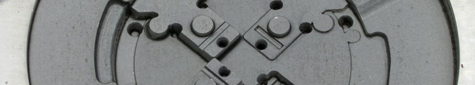
- Automobile industry, e.g. the manufacture of fuel injection valves
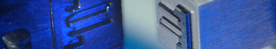
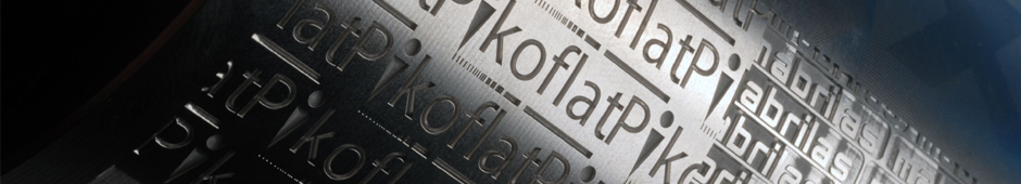
- Tool making and mechanical engineering, e.g. 3D rapid prototyping via ablation
- Scientific, e.g. pumping of dye laser, pumping of OPO and Ti:Saphire laser, particle imaging velocimetry
